

 MRSEC DMR-1420620")
Credits/Names: N. Healy, S. Mailis, N. M. Bulgakova, P. J.-A. Sazio, T.D. Day, J. R. Sparks, J. V. Badding, and A. C. Peacock, Nature Materials (2014) MRSEC DMR-1420620
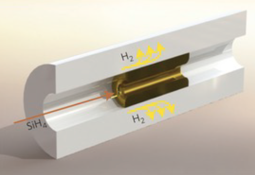
Amorphous silicon wires embedded in silica templates by high-pressure chemical vapor deposition (a technique also used to create ordered 3D metalattices) can be crystallized by a laser. Modeling reveals that shrinkage of the amorphous silicon upon crystallization creates extreme strain in these wires. A combination of experiment and theory suggests that the band gap can change by nearly a factor of two due to this strain. It may thus be possible to employ the technologically versatile silicon platform for detectors at near -IR to mid-IR wavelengths.
Credits/Names: N. Healy, S. Mailis, N. M. Bulgakova, P. J.-A. Sazio, T.D. Day, J. R. Sparks, J. V. Badding, and A. C. Peacock, Nature Materials (2014) MRSEC DMR-1420620
Download PDF Version: Sifiber.pdf
Year of Highlight: 2016
IRG: IRG 3 - High Pressure Enabled Electronic Metalattices